Principle of microcontrollers
The AVR microcontrollers of the Tiny family are characterized by one or two timers. They are Timer0 and Timer1. Usually one of the timers has a simplified set of functions (Timer0) and the second one has an extended set of functions (Timer1). If there is only one timer in a MC, then it has an extended set of functions in most cases.
This timer has an extended set of functions. In the ATtiny 26 microcontroller it is an 8-bit timer like Timer0. The list of functions this node can perform:
Time interval counting.
Generating an interrupt on counter overflow.
Hardware generation Pulse Width Modulated Signal (PWM) (2 channels).
Comparison of the counter with the preset values OCR1A, OCR1B registers, and generating interrupts in case of a match.
Possibility of clocking from system clock generator (fc) (synchronous mode), as well as from internal 64 MHz FALC circuit (fpck). (Asynchronous mode). Structurally, the processor is designed as a single chip (sometimes several).
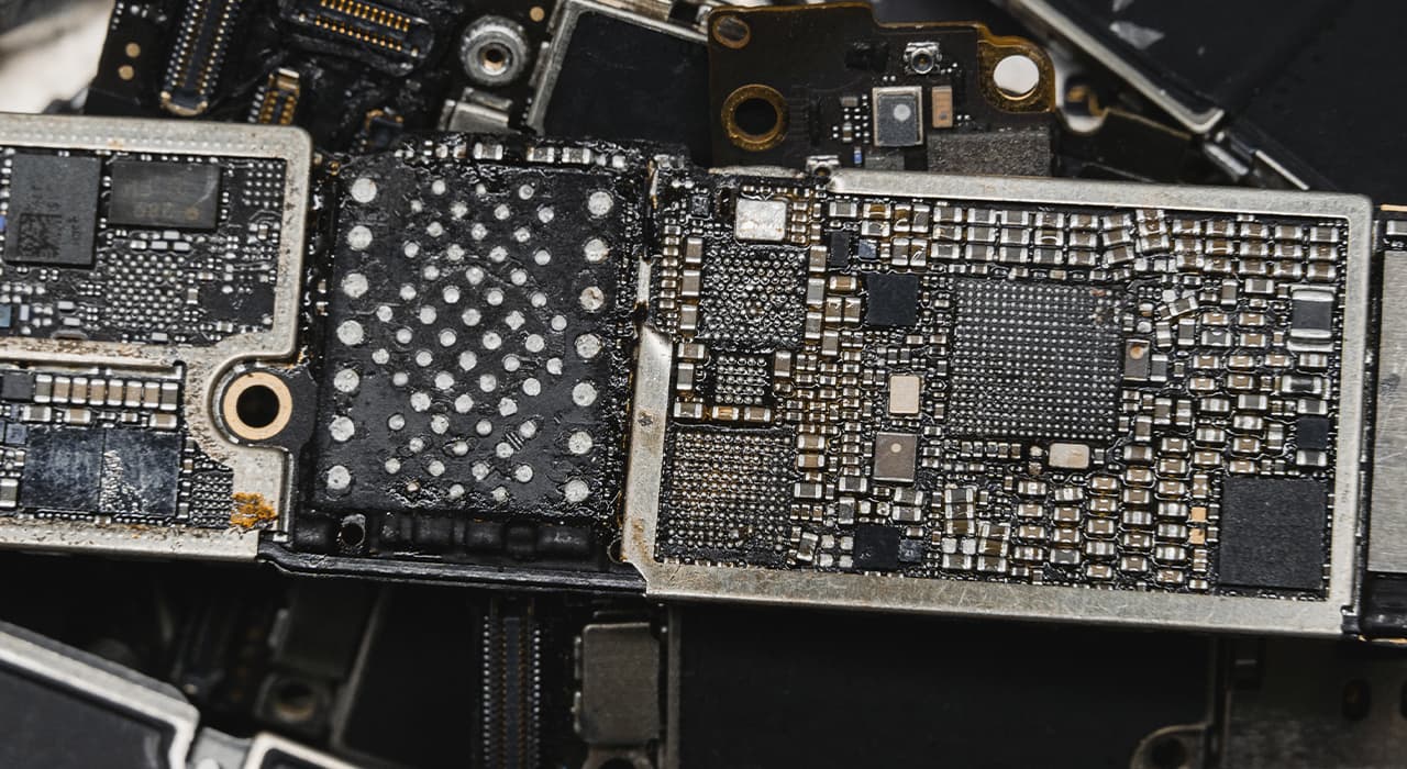
The chip consists of a plastic or ceramic package, which contains a miniature semiconductor substrate inside (Figure 1). On this substrate all electronic circuits of the microprocessor are “drawn” by a laser. The inputs and outputs of the circuit on the substrate are connected to the metal pins located on the sides or bottom of the chip body.
Consider the simplest method – the counter counts in normal mode – cyclically due to overflow. Interrupts are also involved by comparing, say, the register OCR1A. In the overflow interrupt we will turn on the OUT output by feeding log.1 to it. In the Timer1CompA comparison interrupt we will turn the output off by feeding log.0 to it.
So, we will get a sequence of pulses that go with the same period (equal to the counter overflow period, which can be calculated as 256 / ft), where ft is the clocking frequency of the timer. The pulse length will be proportional to the value in the OCR1A register, the larger the value, the later the output will turn off, the longer the pulse will be and the smaller the pause.
Actually the method described is actually software PWM shaping, Timer1 contains a hardware PWM modulator that turns the outputs on and off itself under the conditions described. Interrupt signals are also generated, but usually when operating in PWM mode interrupts from the timer are not used and are prohibited in the control register settings.
To enable the hardware PWM modulator there is a corresponding flag in the control registers. When switching to PWM mode the timer operation is slightly different from the standard mode. Here, by default, the timer does not count to overflow, but to the value that is written in the OCR1C register. When TCNT1 and OCR1C are equal, the counter is reset to 0. This allows accurate pulse frequency setting, it depends not only on the clocking frequency, but also on OCR1C value.
Having two comparison registers OCR1A and OCR1B makes it possible to have two PWM modulator channels (but with the same frequency). So you can easily control two loads of the same type, for example, to change the brightness of two LED lamps independently.
Note that the value of registers OCR1A and OCR1B can range from 0 to OCR1C. Of course, nobody forbids to write there a value greater than OCR1C, but in this case we will have a constant level signal on the output, but not a pulse sequence, because the value of TCNT1 will never reach the condition of equality with the comparison register, according to the signal on the output will not change.
The PWM modulator in the ATTiny 26 has direct outputs OC1A, OC1B as well as inverse outputs OC1A, OC1B. At that the levels on the inverse outputs in PWM mode do not change simultaneously with the change of levels of direct outputs. The transition from 0 to 1 of the inverse pulse occurs one period later than the transition from 1 to 0 on the direct output, and the reverse transition from 1 to 0 on the inverse output occurs earlier by one period than the transition from 0 to 1 on the direct output. The switching of direct and inverse outputs, as well as the order of signal change on them, can be changed by means of control registers. The standard formation of the PWM signal by the timer ATTiny 26 is shown in the figure: It should be noted that the value in the registers OCR1A and OCR1B change when the counter is zeroed. This is hardware implemented with so-called buffer registers, that is, the program can change the value at any time, but writing it to the comparison registers will happen at the moment when the counter goes through 0, until then they are stored in a buffer.